Saturday, June 17, 2017

Basic Electronics on the Go - Active Low Pass Filter

Introduction

Low Pass filter is a filter which passes all frequencies from DC to upper cut-off frequency fH and rejects any signals above this frequency.
In ideal case, the frequency response curve drops at the cut-off frequency. Practically the signal will not drop suddenly but drops gradually from transition region to the stop band region.
Cut-off frequency means the point where the response drops -3 dB or 70.7% from the pass band. Transition region means the area where falloff occurs.
Stop band region means the area where the attenuation occurs mostly to the input signals. So this filter is also called  high-cut filter or treble cut filter. The ideal response is shown below

Rather than the passive components the Active Low Pass Filter is formed by active components like Op-Amps, FETs and transistors. These filters are very effective when compared with the passive filters. Active filters are introduced to overcome the defects of passive filters.

A simple active low pass filter is formed by using an op-amp. The operational amplifier will take the high impedance signal as input and gives a low impedance signal as output. The amplifier component in this filter circuit will increase the output signal amplitude.

By this action of the amplifier the output signal will become wider or narrower. The maximum frequency response of the filter depends on the amplifier used in the circuit design.


Active low pass filter circuit


The attenuation of the signal, that is the amplitude of the output signal is less than amplitude of the input signal in a passive circuit. In order to overcome this disadvantage of the passive filter, the active filter is designed. A Passive filter connected to the inverting or non-inverting op-amp gives us a simple active low pass filter.

First order active filter is formed by a single op-amp with RC circuit. A simple RC Passive Filter connected to the non-inverting terminal of an operational amplifier is shown below


This first-order low pass active filter, consists simply of a passive RC filter stage providing a low frequency path to the input of a non-inverting operational amplifier. The amplifier is configured as a voltage-follower (Buffer) giving it a DC gain of one, Av = +1 or unity gain as opposed to the previous passive RC filter which has a DC gain of less than unity.

The advantage of this configuration is that the op-amps high input impedance prevents excessive loading on the filters output while its low output impedance prevents the filters cut-off frequency point from being affected by changes in the impedance of the load.

While this configuration provides good stability to the filter, its main disadvantage is that it has no voltage gain above one. However, although the voltage gain is unity the power gain is very high as its output impedance is much lower than its input impedance. If a voltage gain greater than one is required we can use the following filter circuit.


Active low pass filter with high voltage gain


When the input signals are at low frequencies the signals will pass through the amplifying circuit directly, but if the input frequency is high the signals are passed through the capacitor C1. By this filter circuit the output signal amplitude is increased by the pass band gain of the filter.


We know that, for non-inverting amplifier circuit the magnitude of the voltage gain is obtained by its feedback resistor  R2 divided by its corresponding input resistor R3.
This is given as follows

Magnitude of the voltage Gain= {1 + (R2/R3)}


Active low pass filter voltage gain

We know that the gain can be obtained by the frequency components and this is given as follows
Voltage gain = V_out⁄V_in = A_max⁄ √(1+〖f/f_c 〗^2 )
Where
  • Amax = Gain of the pass band = 1 + R_2⁄R_3
  • f = operational frequency.
  • fc = Cut-off frequency.
  • Vout = Output voltage.
  • Vin= Input voltage.
When the frequency increases, then the gain decreases by 20 dB for every 10 time increment of frequency. This operation is observed  below
At low frequencies that is when operating frequency f is less than cut-off frequency, then

Vout / Vin = Amax


When operating frequency is equal to the cut off frequency, then
Vout / Vin = Amax / √2 = 0.707 Amax
When the operating frequency is less than the cut off frequency, then
Vout / Vin < Amax

By these equations we can say that at low frequencies the circuit gain is equal to maximum gain and at high frequencies the circuit gain is less than maximum gain Amax.

By these equations we can say that at low frequencies the circuit gain is equal to maximum gain and at high frequencies the circuit gain is less than maximum gain Amax.
When actual frequency is equal to the cut-off frequency, then the gain is equal to the 70.7% of the Amax. By this we can say that for every tenfold (decade) increase of frequency the gain of the voltage is divided by 10.
Magnitude of the Voltage Gain (dB):  Amax = 20 log10 (Vout / Vin)
At -3 dB frequency the gain is given as:
3 dB Amax = 20 log10 {0.707 (Vout / Vin)}


Frequency Response


The response of the active filter is as shown in below figure


Second Order Active Low Pass Filter


Just by adding an additional RC circuit to the first order low pass filter the circuit behaves as a second order filter.The second order filter circuit is shown above.

The gain of the above circuit is  Amax = 1 + (R2/R1)
The cut-off frequency of second order low pass filter is fc = 1 / 2π√(C1C2R3R4)
The frequency response and the designing steps of the second order filter and the first order filter are almost same except the roll off of the stop band. The roll off value of the second order filter is double to that of first order filter that is 40dB/decade or 12dB/octave.


Applications Of Active Low Pass Filters

In electronics these filters are widely used in many applications. These filters are used as hiss filters in audio speakers to reduce the high frequency hiss produced in the system and these are used as inputs for sub woofers.
These are also used in equalisers and audio amplifiers. In analog to digital conversion these are used as anti-aliasing filters to control signals. In digital filters these are used in blurring of images, smoothing sets of data signals. In radio transmitters to block harmonic emissions.

In acoustics these filters are used to filter the high frequency signals from the transmitting sound which will cause echo at higher sound frequencies.


Monday, June 5, 2017

Basic Electronics on the Go - Band Stop Filter

http://www.electronicshub.org/band-stop-filter/


Introduction

The band stop filter is formed by the combination of low pass and high pass filters with a parallel connection instead of cascading connection. The name itself indicates that it will stop a particular band of frequencies. Since it eliminates frequencies, it is also called band elimination filter or band reject filter or notch filter.

We know that unlike high pass and low pass filters, band pass and band stop filters have two cut-off frequencies. It will pass above and below a particular range of frequencies whose cut off frequencies are predetermined depending upon the value of the components used in the circuit design.

Any frequencies in between these two cut-off frequencies are attenuated. It has two pass bands and one stop band. The ideal characteristics of the Band pass filter are as shown below

Where fL indicates the cut off frequency of the low pass filter.
fis the cut off frequency of the high pass filter.
The centre frequencies fc = √( fL x fH)
The characteristics of a band stop filter are exactly opposite of the band pass filter characteristics.
When the input signal is supplied, the low frequencies are passed through the low pass filter in the band stop circuit and the high frequencies are passed through the high pass filter in the circuit. This is shown in the   block diagram below.

In practice, due to the capacitor switching mechanism in the high pass and low pass filter the output characteristics are not same as that of  the ideal filter. The pass band gain must be equal for the low pass filter and high pass filter. The frequency response of band stop filter is shown below and red line indicates the practical response in the  figure below


Band Stop Filter circuit using R, L and C

A simple band stop filter circuit with passive components is shown below


The output is taken across the inductor and capacitor which are connected in series. We know that for different frequencies in the input the circuit behaves either as an open or short circuit. At low frequencies the capacitor acts as an open circuit and the inductor acts like a short circuit. At high frequencies the inductor acts like an open circuit and the capacitor acts like a short circuit.

Thus, by this we can say that at low and high frequencies the circuit acts like an open circuit because inductor and capacitor are connected in series. By this it is also clear that at mid frequencies the circuit acts like a short circuit. Thus the mid frequencies signals are not allowed to pass through the circuit.

The mid frequency range to which the filter acts as a short circuit depends on the values of lower and upper cut-off frequencies. This lower and upper cut-off frequency values depends on the component values. These component values are determined by the transfer functions for the circuit according to the design. The transfer function is nothing but the ratio of the output to the input.

Where angular frequency ω = 2πf


Notch filter (Narrow band stop filter)


The above circuit shows the Twin ‘T’ network. This circuit gives us a notch filter. A notch filter is nothing but a narrow Band stop filter. The characteristic shape of the band stop response makes the filter  a notch filter. This notch filter is applied to eliminate the single frequency. Since it consists of two ‘T’ shaped networks, it is referred to as a Twin T network. The maximum elimination  occurs at the centre frequency  fC = 1/(2πRC).

In order to eliminate the specific value of the frequency in the case of a notch filter, the capacitor chosen in the circuit design must be less than or equal to the 1 µF. By using the centre frequency equation,we can calculate the value of the resistor. By using this notch circuit,we can eliminate single frequency at 50 or 60 Hz.

The second order notch filter with active component op-amp in non-inverting configuration is given as follows


The gain can be calculated as


Where Quality factor Q = 1/ 2 x (2 – Amax)
If the value of the quality factor is high, then the width of the notch filter is narrow.

Frequency Response of the Band Stop Filter

By taking the frequency and gain, the frequency response of the stop band is obtained as shown below

The bandwidth is taken across the lower and higher cut-off frequencies. According to ideal filter the pass band must have the gain as Amax and a stop band must have zero gain. In practice, there will be some transition region. We can measure the pass band ripple and stop band ripples as follows
Pass Band Ripple = – 20 log10(1-δp) dB
Stop Band Ripple = – 20 log10(δs) dB

Where
δp = Magnitude response of the pass band filter.
δs= Magnitude response of the stop band filter.
The typical stop bandwidth of the band stop filter is 1 to 2 decades. The highest frequency eliminated is 10 to 100 times the lowest frequencies eliminated.


Ideal response of the notch filter


Band stop filter summary

Band Stop filter has two pass bands and one stop band. The characteristics of this filter are exactly opposite to the Band Pass Filter. It is also called Band rejection filter or Band elimination filter. It uses a high pass filter and a low pass filter connected in parallel. 
The Band Stop filter with narrow band stop features is called  a notch filter. It is used to eliminate the single frequency value. It is formed by two resistors and two capacitors connected in two ‘T’ shaped networks.

So, it is referred to  as a Twin ‘T’ filter. The bandwidth of the filter is nothing but the stop band of the filter. If the quality factor Q is high, the more  narrow is the width of the notch response. These are widely preferred in communication circuits.


Applications of the Band Stop filter

In different technologies, these filters are used at different varieties.

  • In telephone technology, these filters are used as  telephone line noise reducers  in DSL internet services. It will help to remove the interference on the line which  reduce the DSL performance.
  • These are widely used in the electric guitar amplifiers. Actually,this electric guitar produces a ‘hum’ at 60 Hz frequency. This filter is used to reduce that hum in order to amplify the signal produced by the guitar amplifier. These are also used in some of the acoustic applications like mandolin, base instrument amplifiers.
  • In communication electronics the signal is distorted due to some noise (harmonics) which makes the original signal to interfere with other signals. This leads to errors in the output. Thus, these filters are used to eliminate these unwanted harmonics.
  • These are used to reduce the static on radio, which is commonly used in our daily life.
  • These are also used in Optical communication technologies, at the end of the optical fiber there may be some interfering (spurious) frequencies of light which makes the distortions in the light beam. These distortions are eliminated by band stop filters. The best example is in Raman spectroscopy.
  • In image and signal processing these filters are highly preferred to reject noise.
  • These are used in high quality audio applications like PA systems (Public address systems).
  • These are also used in medical field applications,i.e., in biomedical instruments like EGC for removing line noise.

Friday, May 19, 2017

Basic Electronics on the Go - Passive Band Pass RC Filter

From http://www.electronicshub.org/passive-band-pass-rc-filter/


Introduction

We can say that a Band pass filter is a combination of both low pass filter and high pass filter. The name of the filter itself indicates that it allows only a certain band of frequencies and blocks all the remaining frequencies. In audio applications, sometimes it is necessary to pass only a certain range of frequencies - this frequency range does not start at 0Hz or end at very high frequency but these frequencies are within a certain range, either wide or narrow. These bands of frequencies are commonly termed as Bandwidth.


Passive Band Pass filter

Band pass filter is obtained by cascading passive low pass and passive high pass filters. This arrangement will provide a selective filter which passes only certain frequencies. This new RC filter circuit can pass either a narrow range of frequencies or wide range of frequencies. This range of frequencies that is either narrow or wide range will depend upon the way the passive low pass and high pass filter cascade. The upper and lower cut-off frequencies depend on filter design. This band pass filter is simply  like a frequency selective filter.
The above figure shows the Band pass filter circuit. The input given is a sinusoidal signal. The properties of low pass and high pass combinations give us Band pass filter. By arranging one set of RC elements in series and another set of RC elements in parallel the circuit behaves like a band pass filter. This gives us a second order filter because the circuit has two reactive components. One capacitor belongs to the low pass filter and another capacitor belongs to the high pass filter. Without any variations in the input signal this band pass filter will pass a certain range of frequencies. This filter does not produce any extra noise in the signal. The cut-off frequency of the circuit can be calculated as follows
fC = 1/(2πRC)​


By adjusting the cut-off frequencies of the high pass and low pass filters we can obtain the appropriate width of the pass band for the band pass filter.
Since this filter passes a band of frequencies this filter contains two cut off frequencies, lower cut-off frequency ‘ fL‘ and higher cut-off frequency ‘fH’. Thus the range of the frequencies which are passed through the filter is called as Band Width of the filter. In general the Band Width of the circuit can be calculated by the frequencies ‘fand fL‘.

BW = fH – fL

Where , ‘fH‘ is the cut-off frequency of the high pass filter and  ‘ fL‘ is the cut-off frequency of the low pass filter. ‘BW’ is the bandwidth of the filter. The band pass filter will pass the frequencies higher than the cut off frequency of the high pass filter and lower than the cut off frequency of the low pass filter. This shows that the cut off frequency of the low pass filter must be higher than the cut off frequency of the high pass filter.


Band pass filter using R, L and C components


Band Pass Filter circuit design by using inductor, capacitor and resistor is as shown below


The centre frequency of the band pass filter which is also termed as ‘resonant peak’ can be formulated by using the equation.
fc = 1/2π√(LC)
Where L = inductance of an inductor whose units are in Henry (H).
C = capacitance of a capacitor whose units are in Farad (F).
We can also design a band pass filter with inductors, but we know that due to high reactance of the capacitors, the band pass filter design with RC elements is more advantageous than RL circuits.


The pole frequency is approximately equal to the frequency of the maximum gain.
The frequency response curve of the band pass filter is as shown below: The ideal characteristics and the practical characteristics of the band pass filters are different because of the input reactance of the circuit.


The gain of the input signal can be calculated by taking 20 log (Vout / Vin). The range can be quite large, depending on the  inherent characteristics of the circuit. The signal is attenuated at low frequencies with the output increasing at a slope of +20 dB per decade or 6 dB per octave until the frequency reaches to lower cut off frequency ‘fL’. At this frequency the gain of the signal is at the value 1/√2 = 70.7%.

At maximum gain, the  gain is constant until it reaches the higher cut off frequency ‘f_H’.After the higher cut-off frequency, the output decreases at a slope of -20dB/decade or -6dB/octave.

Previously we have seen that the phase shift of  the first order filter is 90°. We know that the band pass filter is a second order filter so the phase shift is twice of the first order filter that is 180°. The phase angle will vary with the increase of the frequency. At centre frequency the output and input signals are in-phase with each other. Below the resonant frequency the output signal leads the input signal and above the resonantfrequency the output signal lags the input signal. The amplitude of the input signal is always greater than the output signal. In order to increase the gain of the circuit the resistance R1 value must be higher than the resistance R2.

Band Pass Filter Centre Frequency

The “Center frequency” or “Resonant frequency” at which the output gain is maximum can be obtained by calculating the Geometric mean of lower and upper cut-off frequencies.
fr2 = fH x fL
fr = √(fH x fL)
Where fr is the resonant frequency or centre frequency
fH  – is the upper -3 dB cut-off frequency
fL – is the lower -3 dB cut-off frequency


Passive Band Pass Filter Summary

The band pass filter is obtained by cascading a low pass and high pass filter. It is a second order filter since it contains two reactive elements. The order of the filter depends on the number of cascading circuits using in the circuit.
The gain of the output signal is always less than the input signal.At the centre frequency the output signal is in-phase, but below centre frequency the output signal leads the phase with shift of +90° and above centre frequency the output signal will lag in phase with the phase shift of -90°.
The practical characteristics of the band pass filter are a bit different with respect to the ideal characteristics. This variation is mainly due to cascading of high pass filter with low pass filter. The output gain is always less than unity. When we provide electrical isolation between the high pass and low pass filters we can attain better performance of the filter.
The band pass filter will optimize the sensitivity of the receiver. The high pass filter is first added to the design later low pass filter is added. Even though we add a low pass filter first and then the high pass filter, it will never make changes in the output signal. The quality factor of the filter will depend upon the resistor value R1. If R1 is low the quality factor is low and if the R1 value is high then, the quality factor is high.


Applications of Band Pass Filter

1. These are used in wireless communication medium at transmitter and receiver circuits. In transmitter section this filter will pass the only required signals and reduces the interfering of signals with other stations. In the receiver section, it will prevent unwanted signal penetration in to the channels.
2. These are used to optimize the signal to noise ratio of the receiver.

3. These are used in optical communication area like LIDARS.
4. They are used in some of the techniques of colour filtering.
5. These are also used in medical field instruments like EEG.

6. In telephonic applications, at DSL to split phone and broad band signals.


Monday, May 8, 2017

Basic Electronics on the Go - Passive High Pass RC Filters


From http://www.electronicshub.org/passive-high-pass-rc-filters/
From http://www.electronics-tutorials.ws/filter/filter_3.html


Electrical filter is a circuit, designed to reject all unwanted frequency components of an electrical signal and allows only desired frequencies. In other words a filter is a circuit which allows only a certain band of frequencies.
In many applications, capacitive filters are used more than the inductive filters because the inductors will produce some stray magnetic fields and dissipates some amount of power. Not only do they  have these drawbacks but also due to the usage of inductors in the circuit, the filters becomes bulky. In the previous tutorials we have studied basics of filters and passive low pass filter. Now let us see the operation of passive high pass RC filter.

Passive High Pass Filter

The passive High pass Filter is similar to the Passive low pass filter. When the capacitor and resistor positions are interchanged in the circuit of the low pass filter the behaviour of high pass filter is exhibited by the circuit. The capacitor is connected in series with the resistor. The input voltage is applied across the series network but the output is drawn only across the resistor.
High Pass filter allows the frequencies which are higher than the cut off frequency ‘fc’ and blocks the lower frequency signals. The value of the cut off frequency depends on the component values chosen for the circuit design. These high pass filters have many applications at high frequency ranges of 10 MHz.
The circuit of the high pass filter is shown below


Due to this interchange of components in the circuit, the responses delivered by the capacitor changes and these changes are exactly opposite to the response of the low pass filter. The capacitor at the low frequencies acts like an open circuit and at higher frequencies which means at the frequencies higher than the cut off frequency capacitor acts like a short circuit. The capacitor will block the lower frequencies entering into the capacitor due to the capacitive reactance of the capacitor.

We know that the capacitor itself opposes some amount of current through it in order to bind within the capacitance range of the capacitor. After the cut off frequency, the capacitor allows all the frequencies because of the reduction of the capacitive reactance value. This makes the circuit pass the entire input signal to the output when input signal frequency is greater than the cut-off frequency fc. At lower frequencies the reactance value increases thus when reactance increases, the ability to oppose the current flow through the capacitor increases.The band of frequencies below the cut off frequency is referred as ‘Stop Band’ and the band of frequencies after the cut off frequency is referred as ‘Pass Band’.

In the above circuit there is only one reactive component with resistor this shows the circuit is first order circuit.

Frequency Response of high pass filter

The response curves with respect to frequency and the capacitive reactance are given below:
This response curve shows that the high pass filter is exactly opposite to the low pass filter. In high pass filter till the cut off frequency, all the low frequency signals are blocked by the capacitor resulting in the decrease of output voltage. At the cut off frequency point, the value of the resistor ‘R’ and the reactance of the capacitor ‘X_c’are equal thus the output voltage increases at a rate of -20 dB/decade and the output signal levels are -3 dB of the input signal levels.

At very high frequencies the capacitive reactance becomes zero then the output voltage is same as that of the input voltage that is Vout = Vin. At low frequencies the capacitive reactance is infinity and thus the output voltage is zero because the reactance will block the current entering in to the capacitor.

The output of the high pass filter has the phase shift angle (ø) of +45° at cut-off frequency with respect to input signal.This shows that the output of the high pass filter  leads with reference to the input signal. At high frequencies (f > fC) the phase shift is almost zero meaning both input and output signals are in phase. 

The time taken by the capacitor for charging and discharging of the plates with respect to the input signal results in a phase difference. The resistor in  series with the capacitor will produce the charging and discharging effect. The time constant of a series RC circuit is defined as the time taken by the capacitor to charge up to 63.2% of the final steady state value and is also  defined as the time taken by the capacitor to discharge to 36.8% of steady state value. This is represented by the symbol’τ’. The relationship between the time constant and the cut off frequency is given as follows

Time constant τ=RC= 1⁄2πfc and ω_c= 1/τ = 1/RC.

By this it is clear that the output of the filter depends on the frequencies applied at the input and time constant.
Cut off frequency and the Phase shift
The Cut off frequency or Break point ‘fc’ = 1/ 2πfc
The phase shift (ø) = tan-1 (2πfRc)


High pass RC filter output voltage and gain


Second Order Passive High Pass Filter


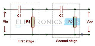
By cascading two first order high pass filters, we get a  second order high pass filter. Since it consists of two reactive components that mean two capacitors, it makes the circuit a second order. The performance of this two stage filter is equal to single stage filter but the slope of the filter is obtained at -40 dB/ decade. This is because of the cut off frequency variation. It is more efficient when compared with the single stage high pass filter because it has two storage points. For two stage filter the cut off frequency will depend on the values of two capacitors and two resistors. This is given as follows
fc = 1/ (2π√(R1C1R2C2)) Hz​

Passive High Pass Filter Summary


The high pass filter allows the frequencies greater than the cut off frequency up to infinity. In practical situations infinity does not exists so this infinity value is dependent on the components used in the circuit design.

The band of frequencies allowed by the High pass filter is referred to  as ‘Pass Band’ and this pass band is nothing but the bandwidth of the filter. The band of frequencies attenuated by the filter is known as ‘stop band’.
The cut off frequency is calculated by using the formula ‘fc’ which is shown above. The phase shift of the output signal is leading the input signal with an angle of +45°. The output voltage will depends on the time constant and the input frequency applied to the circuit. The distortions eliminated by the high pass filters are more accurate when compared with the low pass filters because of the high frequencies used in the circuit.


High pass RC Differentiator

For normal sinusoidal wave inputs the performance of the filter is just like the first order high pass filter But when we apply different type of signals rather than the sine waves such as square waves which gives time domain response such as step or impulse as the input signal then the circuit behaves like a Differentiator circuit. A circuit whose derivative of the input is directly proportional to the output of the circuit is called a Differentiator circuit.


Thus when constant input is applied to the circuit the output becomes zero because the derivative of the constant tends to zero.

RC Differential circuit is shown below.

For square wave input signals, the output wave form appears as  short duration pulses. For one complete cycle of input, there are two spike signals with positive and negative pulses. In this process there will be no change in the amplitude of the output signal. If the input signal frequency increases then the width of the pulse at the output increases. The rate of the decay of the spike pulse depends on the time constant.


Applications of the High Pass Filter


  • These are used in  audio amplifiers as a coupling capacitor between two audio amplifier stages and in speaker systems to direct the higher frequency signals to the smaller “tweeter” type speakers while blocking the lower bass signals 
  • These are used as rumble filters to block the nearby unwanted signals and pass the required signals in the loud speakers.
  • These are used in the AC coupling circuits and as  differentiator circuits.
  • In the mixing process at each channel strips, these high pass filters are added.
  • In  image processing, the high pass filters are used in the process of unsharpening where editing requires a high boosting filter.
  • In  image processing, the reduction of noise can be done in either time domain or in the frequency domain. So combining with the low pass filters, these high pass filters are used to enhance, noise suppression and modify the images in the image processing.