Thursday, July 26, 2018

Basic Electronics on the Go - The Light Emitting Diode

From https://www.electronics-tutorials.ws/diode/diode_8.html

 The Light Emitting Diode

 Light Emitting Diodes or simply LED´s, are among the most widely used of all the different types of semiconductor diodes available today and are commonly used in TV’s and colour displays.

 They emit a fairly narrow bandwidth of either visible light at different coloured wavelengths, invisible infra-red light for remote controls or laser type light when a forward current is passed through them.

The “Light Emitting Diode” or LED as it is more commonly called, is basically just a specialised type of diode as they have very similar electrical characteristics to a PN junction diode. This means that an LED will pass current in its forward direction but block the flow of current in the reverse direction.

Light emitting diodes are made from a very thin layer of fairly heavily doped semiconductor material and depending on the semiconductor material used and the amount of doping, when forward biased an LED will emit a coloured light at a particular spectral wavelength.

 When the diode is forward biased, electrons from the semiconductors conduction band recombine with holes from the valence band releasing sufficient energy to produce photons which emit a monochromatic (single colour) of light. Because of this thin layer a reasonable number of these photons can leave the junction and radiate away producing a coloured light output.


Then we can say that when operated in a forward biased direction Light Emitting Diodes are semiconductor devices that convert electrical energy into light energy.
The construction of a Light Emitting Diode is very different from that of a normal signal diode. The PN junction of an LED is surrounded by a transparent, hard plastic epoxy resin hemispherical shaped shell or body which protects the LED from both vibration and shock.


light emitting diode construction


Surprisingly, an LED junction does not actually emit that much light so the epoxy resin body is constructed in such a way that the photons of light emitted by the junction are reflected away from the surrounding substrate base to which the diode is attached and are focused upwards through the domed top of the LED, which itself acts like a lens concentrating the amount of light. This is why the emitted light appears to be brightest at the top of the LED.

However, not all LEDs are made with a hemispherical shaped dome for their epoxy shell. Some indication LEDs have a rectangular or cylindrical shaped construction that has a flat surface on top or their body is shaped into a bar or arrow. Generally, all LED’s are manufactured with two legs protruding from the bottom of the body.

Also, nearly all modern light emitting diodes have their cathode, (  ) terminal identified by either a notch or flat spot on the body or by the cathode lead being shorter than the other.

 Unlike normal incandescent lamps and bulbs which generate large amounts of heat when illuminated, the light emitting diode produces a “cold” generation of light which leads to higher efficiencies than the normal “light bulb” because most of the generated energy radiates away within the visible spectrum. Because LEDs are solid-state devices, they can be extremely small and durable and provide much longer lamp life than normal light sources.

Light Emitting Diode Colours

So how does a light emitting diode get its colour. Unlike normal signal diodes which are made for detection or power rectification, and which are made from either Germanium or Silicon semiconductor materials, Light Emitting Diodes are made from exotic semiconductor compounds such as Gallium Arsenide (GaAs), Gallium Phosphide (GaP), Gallium Arsenide Phosphide (GaAsP), Silicon Carbide (SiC) or Gallium Indium Nitride (GaInN) all mixed together at different ratios to produce a distinct wavelength of colour.

Different LED compounds emit light in specific regions of the visible light spectrum and therefore produce different intensity levels. The exact choice of the semiconductor material used will determine the overall wavelength of the photon light emissions and therefore the resulting colour of the light emitted.


Light Emitting Diode Colours

Typical LED Characteristics
Semiconductor
Material
Wavelength Colour VF @ 20mA
GaAs 850-940nm Infra-Red 1.2v
GaAsP 630-660nm Red 1.8v
GaAsP 605-620nm Amber 2.0v
GaAsP:N 585-595nm Yellow 2.2v
AlGaP 550-570nm Green 3.5v
SiC 430-505nm Blue 3.6v
GaInN 450nm White 4.0v

Therefore the colour of the light emitted by an LED is NOT determined by the colouring of the LED’s plastic body although these are slightly coloured to both enhance the light output and to indicate its colour when its not being illuminated by an electrical supply.

Light emitting diodes are available in a wide range of colours with the most common being RED, AMBER,  YELLOW  and GREEN and are thus widely used as visual indicators and as moving light displays.
Recently developed blue and white coloured LEDs are also available but these tend to be much more expensive than the normal standard colours due to the production costs of mixing together two or more complementary colours at an exact ratio within the semiconductor compound and also by injecting nitrogen atoms into the crystal structure during the doping process.
From the table above we can see that the main P-type dopant used in the manufacture of Light Emitting Diodes is Gallium (Ga, atomic number 31) and that the main N-type dopant used is Arsenic (As, atomic number 33) giving the resulting compound of Gallium Arsenide (GaAs) crystalline structure.
The problem with using Gallium Arsenide on its own as the semiconductor compound is that it radiates large amounts of low brightness infra-red radiation (850nm-940nm approx.) from its junction when a forward current is flowing through it.
The amount of infra-red light it produces is okay for television remote controls but not very useful if we want to use the LED as an indicating light. But by adding Phosphorus (P, atomic number 15), as a third dopant the overall wavelength of the emitted radiation is reduced to below 680nm giving visible red light to the human eye. Further refinements in the doping process of the PN junction have resulted in a range of colours spanning the spectrum of visible light as we have seen above as well as infra-red and ultra-violet wavelengths.


By mixing together a variety of semiconductor, metal and gas compounds the following list of LEDs can be produced.

Types of Light Emitting Diode

  • Gallium Arsenide (GaAs) – infra-red
  • Gallium Arsenide Phosphide (GaAsP) – red to infra-red, orange
  • Aluminium Gallium Arsenide Phosphide (AlGaAsP) – high-brightness red, orange-red, orange, and yellow
  • Gallium Phosphide (GaP) – red, yellow and green
  • Aluminium Gallium Phosphide (AlGaP) – green
  • Gallium Nitride (GaN) – green, emerald green
  • Gallium Indium Nitride (GaInN) – near ultraviolet, bluish-green and blue
  • Silicon Carbide (SiC) – blue as a substrate
  • Zinc Selenide (ZnSe) – blue
  • Aluminium Gallium Nitride (AlGaN) – ultraviolet
Like conventional PN junction diodes, light emitting diodes are current-dependent devices with its forward voltage drop VF, depending on the semiconductor compound (its light colour) and on the forward biased LED current. Most common LED’s require a forward operating voltage of between approximately 1.2 to 3.6 volts with a forward current rating of about 10 to 30 mA, with 12 to 20 mA being the most common range.
Both the forward operating voltage and forward current vary depending on the semiconductor material used but the point where conduction begins and light is produced is about 1.2V for a standard red LED to about 3.6V for a blue LED.
The exact voltage drop will of course depend on the manufacturer because of the different dopant materials and wavelengths used. The voltage drop across the LED at a particular current value, for example 20mA, will also depend on the initial conduction VF point. As an LED is effectively a diode, its forward current to voltage characteristics curves can be plotted for each diode colour as shown below.


Light Emitting Diodes I-V Characteristics.

light emitting diode 


 ight Emitting Diode (LED) Schematic symbol and I-V Characteristics Curves
showing the different colours available.

Before a light emitting diode can “emit” any form of light it needs a current to flow through it, as it is a current dependant device with their light output intensity being directly proportional to the forward current flowing through the LED.
As the LED is to be connected in a forward bias condition across a power supply it should be current limited using a series resistor to protect it from excessive current flow. Never connect an LED directly to a battery or power supply as it will be destroyed almost instantly because too much current will pass through and burn it out.


From the table above we can see that each LED has its own forward voltage drop across the PN junction and this parameter which is determined by the semiconductor material used, is the forward voltage drop for a specified amount of forward conduction current, typically for a forward current of 20mA.
In most cases LEDs are operated from a low voltage DC supply, with a series resistor, RS used to limit the forward current to a safe value from say 5mA for a simple LED indicator to 30mA or more where a high brightness light output is needed.


LED Series Resistance.

The series resistor value RS is calculated by simply using Ohm´s Law, by knowing the required forward current IF of the LED, the supply voltage VS across the combination and the expected forward voltage drop of the LED, VF at the required current level, the current limiting resistor is calculated as:

LED Series Resistor Circuit

 light emitting diode circuit


Light Emitting Diode Example No1

An amber coloured LED with a forward volt drop of 2 volts is to be connected to a 5.0v stabilised DC power supply. Using the circuit above calculate the value of the series resistor required to limit the forward current to less than 10mA. Also calculate the current flowing through the diode if a 100Ω series resistor is used instead of the calculated first.
1). series resistor required at 10mA.

light emitting diode series resistor

2). with a 100Ω series resistor.

led current

We remember from the Resistors tutorials, that resistors come in standard preferred values. Our first calculation above shows that to limit the current flowing through the LED to 10mA exactly, we would require a 300Ω resistor. In the E12 series of resistors there is no 300Ω resistor so we would need to choose the next highest value, which is 330Ω. A quick re-calculation shows the new forward current value is now 9.1mA, and this is ok.


Connecting LEDs Together in Series

We can connect LED’s together in series to increase the number required or to increase the light level when used in displays. As with series resistors, LED’s connected in series all have the same forward current, IF flowing through them as just one. As all the LEDs connected in series pass the same current it is generally best if they are all of the same colour or type.

Connecting LED’s in Series


 leds connected in series


Although the LED series chain has the same current flowing through it, the series voltage drop across them needs to be considered when calculating the required resistance of the current limiting resistor, RS. If we assume that each LED has a voltage drop across it when illuminated of 1.2 volts, then the voltage drop across all three will be 3 x 1.2v = 3.6 volts.
If we also assume that the three LEDs are to be illuminated from the same 5 volt logic device or supply with a forward current of about 10mA, the same as above. Then the voltage drop across the resistor, RS and its resistance value will be calculated as:

series led current limiting resistor

Again, in the E12 (10% tolerance) series of resistors there is no 140Ω resistor so we would need to choose the next highest value, which is 150Ω.


LED Driver Circuits

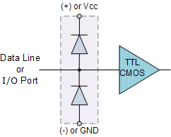
Now that we know what is an LED, we need some way of controlling it by switching it “ON” and “OFF”. The output stages of both TTL and CMOS logic gates can both source and sink useful amounts of current therefore can be used to drive an LED. Normal integrated circuits (ICs) have an output drive current of up to 50mA in the sink mode configuration, but have an internally limited output current of about 30mA in the source mode configuration.

Either way the LED current must be limited to a safe value using a series resistor as we have already seen. Below are some examples of driving light emitting diodes using inverting ICs but the idea is the same for any type of integrated circuit output whether combinational or sequential.


IC Driver Circuit

led driver circuit

If more than one LED requires driving at the same time, such as in large LED arrays, or the load current is too high for the integrated circuit or we may just want to use discrete components instead of ICs, then an alternative way of driving the LEDs using either bipolar NPN or PNP transistors as switches is given below. Again as before, a series resistor, RS is required to limit the LED current.


Transistor Driver Circuit

led transistor driver


The brightness of a light emitting diode cannot be controlled by simply varying the current flowing through it. Allowing more current to flow through the LED will make it glow brighter but will also cause it to dissipate more heat. LEDs are designed to produce a set amount of light operating at a specific forward current ranging from about 10 to 20mA.
In situations where power savings are important, less current may be possible. However, reducing the current to below say 5mA may dim its light output too much or even turn the LED “OFF” completely. A much better way to control the brightness of LEDs is to use a control process known as “Pulse Width Modulation” or PWM, in which the LED is repeatedly turned “ON” and “OFF” at varying frequencies depending upon the required light intensity of the LED.


LED Light Intensity using PWM


 pwm light control

When higher light outputs are required, a pulse width modulated current with a fairly short duty cycle (“ON-OFF” Ratio) allows the diode current and therefore the output light intensity to be increased significantly during the actual pulses, while still keeping the LEDs “average current level” and power dissipation within safe limits.
This “ON-OFF” flashing condition does not affect what is seen by the human eye as it “fills” in the gaps between the “ON” and “OFF” light pulses, providing the pulse frequency is high enough, making it appear as a continuous light output. So pulses at a frequency of 100Hz or more actually appear brighter to the eye than a continuous light of the same average intensity.

(to be updated)

Wednesday, April 11, 2018

C on the go - 3- \n to set a new line

Video:- https://www.youtube.com/watch?v=aRAg1tJItn8


References: https://www.tutorialspoint.com/learn_c_by_examples/index.htm
                    https://www.learn-c.org/en

 
Notes:-

  printf( "Hello, World\n" ); //we will need to call the function printf to print our sentence. \n is used to set a new line

   int op1, op2, sum, sub;      // variable declaration

   op1 = 5;                // variable definition
   op2 = 3;

   sum = op1 + op2;        // addition operation

   printf("sum of %d and %d is %d", op1, op2, sum);


Check out the C programming playlist at https://www.youtube.com/playlist?list=PLDMwfcFQi85p0B1w3o6gLaVQ6eOkCHJz5

C on the go - 2- Variables

Video:-  https://www.youtube.com/watch?v=d9bWO9DASjQ

References: https://www.tutorialspoint.com/learn_c_by_examples/index.htm
                    https://www.learn-c.org/en

Notes:-

int op1, op2, sum;      // variable declaration

   op1 = 5;                // variable definition
   op2 = 3;

   sum = op1 + op2;        // addition operation

printf("sum of %d and %d is %d", op1, op2, sum);

Tuesday, April 10, 2018

C on the go - 1- 'Hello World'

Video -  https://www.youtube.com/watch?v=MPp09MgBaKA
References:- https://www.tutorialspoint.com/learn_c_by_examples/index.htm
                    https://www.learn-c.org/en

Notes:-

 //include library called stdio.h

 int main() //code which will run will always reside in the main function. The int keyword indicates that the function main will return an integer - a simple number, in this case 0

 printf( "Hello, World" ); //we will need to call the function printf to print our sentence.
 
 return 0;

Saturday, April 7, 2018

Basic Electronics on the Go - The Zener Diode

From https://www.electronics-tutorials.ws/diode/diode_7.html

 A Semiconductor Diode blocks current in the reverse direction, but will suffer from premature breakdown or damage if the reverse voltage applied across becomes too high


However, the Zener Diode or “Breakdown Diode”, as they are sometimes referred too, are basically the same as the standard PN junction diode but they are specially designed to have a low and specified Reverse Breakdown Voltage which takes advantage of any reverse voltage applied to it.

The Zener diode behaves just like a normal general-purpose diode consisting of a silicon PN junction and when biased in the forward direction, that is Anode positive with respect to its Cathode, it behaves just like a normal signal diode passing the rated current.

However, unlike a conventional diode that blocks any flow of current through itself when reverse biased, that is the Cathode becomes more positive than the Anode, as soon as the reverse voltage reaches a pre-determined value, the zener diode begins to conduct in the reverse direction.
 
This is because when the reverse voltage applied across the zener diode exceeds the rated voltage of the device a process called Avalanche Breakdown occurs in the semiconductor depletion layer and a current starts to flow through the diode to limit this increase in voltage.

The current now flowing through the zener diode increases dramatically to the maximum circuit value (which is usually limited by a series resistor) and once achieved, this reverse saturation current remains fairly constant over a wide range of reverse voltages. The voltage point at which the voltage across the zener diode becomes stable is called the “zener voltage”, ( Vz ) and for zener diodes this voltage can range from less than one volt to a few hundred volts.

 The point at which the zener voltage triggers the current to flow through the diode can be very accurately controlled (to less than 1% tolerance) in the doping stage of the diodes semiconductor construction giving the diode a specific zener breakdown voltage, ( Vz ) for example, 4.3V or 7.5V. This zener breakdown voltage on the I-V curve is almost a vertical straight line.


Zener Diode I-V Characteristics

zener diode characteristics

The Zener Diode is used in its “reverse bias” or reverse breakdown mode, i.e. the diodes anode connects to the negative supply. From the I-V characteristics curve above, we can see that the zener diode has a region in its reverse bias characteristics of almost a constant negative voltage regardless of the value of the current flowing through the diode and remains nearly constant even with large changes in current as long as the zener diodes current remains between the breakdown current IZ(min) and the maximum current rating IZ(max).

This ability to control itself can be used to great effect to regulate or stabilise a voltage source against supply or load variations. The fact that the voltage across the diode in the breakdown region is almost constant turns out to be an important characteristic of the zener diode as it can be used in the simplest types of voltage regulator applications.

The function of a regulator is to provide a constant output voltage to a load connected in parallel with it in spite of the ripples in the supply voltage or the variation in the load current and the zener diode will continue to regulate the voltage until the diodes current falls below the minimum IZ(min) value in the reverse breakdown region.


The Zener Diode Regulator

Zener Diodes can be used to produce a stabilised voltage output with low ripple under varying load current conditions. By passing a small current through the diode from a voltage source, via a suitable current limiting resistor (RS), the zener diode will conduct sufficient current to maintain a voltage drop of Vout.

We remember from the previous tutorials that the DC output voltage from the half or full-wave rectifiers contains ripple superimposed onto the DC voltage and that as the load value changes so to does the average output voltage. By connecting a simple zener stabiliser circuit as shown below across the output of the rectifier, a more stable output voltage can be produced.

 zener diode regulator


The resistor, RS is connected in series with the zener diode to limit the current flow through the diode with the voltage source, VS being connected across the combination. The stabilised output voltage Vout is taken from across the zener diode. The zener diode is connected with its cathode terminal connected to the positive rail of the DC supply so it is reverse biased and will be operating in its breakdown condition.  

With no load connected to the circuit, the load current will be zero, ( IL = 0 ), and all the circuit current passes through the zener diode which in turn dissipates its maximum power. Also a small value of the series resistor RS will result in a greater diode current and this will increase the power dissipation requirement of the diode so care must be taken when selecting the appropriate value of series resistance so that the zener’s maximum power rating is not exceeded under this no-load or high-impedance condition.


The load is connected in parallel with the zener diode, so the voltage across RL is always the same as the zener voltage, ( VR = VZ ). There is a minimum zener current for which the stabilization of the voltage is effective and the zener current must stay above this value operating under load within its breakdown region at all times. The upper limit of current is of course dependant upon the power rating of the device. The supply voltage VS must be greater than VZ.

One small problem with zener diode stabiliser circuits is that the diode can sometimes generate electrical noise on top of the DC supply as it tries to stabilise the voltage. Normally this is not a problem for most applications but the addition of a large value decoupling capacitor across the zener’s output may be required to give additional smoothing.

 Then to summarise a little. A zener diode is always operated in its reverse biased condition. A voltage regulator circuit can be designed using a zener diode to maintain a constant DC output voltage across the load in spite of variations in the input voltage or changes in the load current. The zener voltage regulator consists of a current limiting resistor RS connected in series with the input voltage VS with the zener diode connected in parallel with the load RL in this reverse biased condition. The stabilized output voltage is always selected to be the same as the breakdown voltage VZ of the diode.


Zener Diode Voltages

As well as producing a single stabilised voltage output, zener diodes can also be connected together in series along with normal silicon signal diodes to produce a variety of different reference voltage output values as shown below.

Zener Diodes Connected in Series

 zener diode reference voltage


 The values of the individual Zener diodes can be chosen to suit the application while the silicon diode will always drop about 0.6 – 0.7V in the forward bias condition. The supply voltage, Vin must of course be higher than the largest output reference voltage and in our example above this is 19v.

A typical zener diode for general electronic circuits is the 500mW, BZX55 series or the larger 1.3W, BZX85 series were the zener voltage is given as, for example, C7V5 for a 7.5V diode giving a diode reference number of BZX55C7V5.

The 500mW series of zener diodes are available from about 2.4 up to about 100 volts and typically have the same sequence of values as used for the 5% (E24) resistor series with the individual voltage ratings for these small but very useful diodes are given in the table below.


Zener Diode Standard Zener Voltages

BZX55 Zener Diode Power Rating 500mW
2.4V 2.7V 3.0V 3.3V 3.6V 3.9V 4.3V 4.7V
5.1V 5.6V 6.2V 6.8V 7.5V 8.2V 9.1V 10V
11V 12V 13V 15V 16V 18V 20V 22V
24V 27V 30V 33V 36V 39V 43V 47V
BZX85 Zener Diode Power Rating 1.3W
3.3V 3.6V 3.9V 4.3V 4.7V 5.1V 5.6 6.2V
6.8V 7.5V 8.2V 9.1V 10V 11V 12V 13V
15V 16V 18V 20V 22V 24V 27V 30V
33V 36V 39V 43V 47V 51V 56V 62V

Zener Diode Clipping Circuits

Thus far we have looked at how a zener diode can be used to regulate a constant DC source but what if the input signal was not steady state DC but an alternating AC waveform how would the zener diode react to a constantly changing signal.

Diode clipping and clamping circuits are circuits that are used to shape or modify an input AC waveform (or any sinusoid) producing a differently shape output waveform depending on the circuit arrangement. Diode clipper circuits are also called limiters because they limit or clip-off the positive (or negative) part of an input AC signal. As zener clipper circuits limit or cut-off part of the waveform across them, they are mainly used for circuit protection or in waveform shaping circuits.

 For example, if we wanted to clip an output waveform at +7.5V, we would use a 7.5V zener diode. If the output waveform tries to exceed the 7.5V limit, the zener diode will “clip-off” the excess voltage from the input producing a waveform with a flat top still keeping the output constant at +7.5V. Note that in the forward bias condition a zener diode is still a diode and when the AC waveform output goes negative below -0.7V, the zener diode turns “ON” like any normal silicon diode would and clips the output at -0.7V as shown below.

Square Wave Signal

 zener diode square wave signal

 If we wanted to clip an output waveform between two different minimum and maximum values of say, +8V and -6V, we would simply use two differently rated zener diodes. Note that the output will actually clip the AC waveform between +8.7V and -6.7V due to the addition of the forward biasing diode voltage.

In other words a peak-to-peak voltage of 15.4 volts instead of expected 14 volts, as the forward bias volt drop across the diode adds another 0.7 volts in each direction.

This type of clipper configuration is fairly common for protecting an electronic circuit from over voltage. The two zener’s are generally placed across the power supply input terminals and during normal operation, one of the zener diodes is “OFF” and the diodes have little or no affect. However, if the input voltage waveform exceeds its limit, then the zener’s turn “ON” and clip the input to protect the circuit.

In the next tutorial about diodes, we will look at using the forward biased PN junction of a diode to produce light. We know from the previous tutorials that when charge carriers move across the junction, electrons combine with holes and energy is lost in the form of heat, but also some of this energy is dissipated as photons but we can not see them.

 If we place a translucent lens around the junction, visible light will be produced and the diode becomes a light source. This effect produces another type of diode known commonly as the Light Emitting Diode which takes advantage of this light producing characteristic to emit light (photons) in a variety of colours and wavelengths.


Saturday, February 24, 2018

Basic Electronics on the Go - Full Wave Rectifier

From https://www.electronics-tutorials.ws/diode/diode_6.html

Power Diodes can be connected together to form a full wave rectifier that convert AC voltage into pulsating DC voltage for use in power supplies.

In the previous Power Diodes tutorial we discussed ways of reducing the ripple or voltage variations on a direct DC voltage by connecting smoothing capacitors across the load resistance.
While this method may be suitable for low power applications it is unsuitable to applications which need a “steady and smooth” DC supply voltage. One method to improve on this is to use every half-cycle of the input voltage instead of every other half-cycle. The circuit which allows us to do this is called a Full Wave Rectifier.

Like the half wave circuit, a full wave rectifier circuit produces an output voltage or current which is purely DC or has some specified DC component. Full wave rectifiers have some fundamental advantages over their half wave rectifier counterparts. The average (DC) output voltage is higher than for half wave, the output of the full wave rectifier has much less ripple than that of the half wave rectifier producing a smoother output waveform.

 In a Full Wave Rectifier circuit two diodes are now used, one for each half of the cycle. A multiple winding transformer is used whose secondary winding is split equally into two halves with a common centre tapped connection, (C). This configuration results in each diode conducting in turn when its anode terminal is positive with respect to the transformer centre point C producing an output during both half-cycles, twice that for the half wave rectifier so it is 100% efficient as shown below.


Full Wave Rectifier Circuit

 The smoothing capacitor converts the full-wave rippled output of the rectifier into a more smooth DC output voltage. If we now run the Partsim Simulator Circuit with different values of smoothing capacitor installed, we can see the effect it has on the rectified output waveform as shown.


Partsim Simulation Waveform


  As the spaces between each half-wave developed by each diode is now being filled in by the other diode the average DC output voltage across the load resistor is now double that of the single half-wave rectifier circuit and is about  0.637Vmax  of the peak voltage, assuming no losses.


Where: VMAX is the maximum peak value in one half of the secondary winding and VRMS is the rms value.

The peak voltage of the output waveform is the same as before for the half-wave rectifier provided each half of the transformer windings have the same rms voltage value. To obtain a different DC voltage output different transformer ratios can be used.

The main disadvantage of this type of full wave rectifier circuit is that a larger transformer for a given power output is required with two separate but identical secondary windings making this type of full wave rectifying circuit costly compared to the “Full Wave Bridge Rectifier” circuit equivalent.

The Full Wave Bridge Rectifier

Another type of circuit that produces the same output waveform as the full wave rectifier circuit above, is that of the Full Wave Bridge Rectifier. This type of single phase rectifier uses four individual rectifying diodes connected in a closed loop “bridge” configuration to produce the desired output.

The main advantage of this bridge circuit is that it does not require a special centre tapped transformer, thereby reducing its size and cost. The single secondary winding is connected to one side of the diode bridge network and the load to the other side as shown below.

The Diode Bridge Rectifier


The four diodes labelled D1 to D4 are arranged in “series pairs” with only two diodes conducting current during each half cycle. During the positive half cycle of the supply, diodes D1 and D2 conduct in series while diodes D3 and D4 are reverse biased and the current flows through the load as shown below.
 

The Positive Half-cycle


 During the negative half cycle of the supply, diodes D3 and D4 conduct in series, but diodes D1 and D2 switch “OFF” as they are now reverse biased. The current flowing through the load is the same direction as before.
 

The Negative Half-cycle


As the current flowing through the load is unidirectional, so the voltage developed across the load is also unidirectional the same as for the previous two diode full-wave rectifier, therefore the average DC voltage across the load is 0.637Vmax.
 
However in reality, during each half cycle the current flows through two diodes instead of just one so the amplitude of the output voltage is two voltage drops ( 2*0.7 = 1.4V ) less than the input VMAX amplitude. The ripple frequency is now twice the supply frequency (e.g. 100Hz for a 50Hz supply or 120Hz for a 60Hz supply.)

Although we can use four individual power diodes to make a full wave bridge rectifier, pre-made bridge rectifier components are available “off-the-shelf” in a range of different voltage and current sizes that can be soldered directly into a PCB circuit board or be connected by spade connectors.


 The image above shows a typical single phase bridge rectifier with one corner cut off. This cut-off corner indicates that the terminal nearest to the corner is the positive or +ve output terminal or lead with the opposite (diagonal) lead being the negative or -ve output lead. The other two connecting leads are for the input alternating voltage from a transformer secondary winding.

The Smoothing Capacitor

We saw in the previous section that the single phase half-wave rectifier produces an output wave every half cycle and that it was not practical to use this type of circuit to produce a steady DC supply. The full-wave bridge rectifier however, gives us a greater mean DC value (0.637 Vmax) with less superimposed ripple while the output waveform is twice that of the frequency of the input supply frequency.
We can improve the average DC output of the rectifier while at the same time reducing the AC variation of the rectified output by using smoothing capacitors to filter the output waveform. Smoothing or reservoir capacitors connected in parallel with the load across the output of the full wave bridge rectifier circuit increases the average DC output level even higher as the capacitor acts like a storage device as shown below.

Full-wave Rectifier with Smoothing Capacitor


 The smoothing capacitor converts the full-wave rippled output of the rectifier into a more smooth DC output voltage. If we now run the Partsim Simulator Circuit with different values of smoothing capacitor installed, we can see the effect it has on the rectified output waveform as shown.

5uF Smoothing Capacitor


 The blue plot on the waveform shows the result of using a 5.0uF smoothing capacitor across the rectifiers output. Previously the load voltage followed the rectified output waveform down to zero volts. Here the 5uF capacitor is charged to the peak voltage of the output DC pulse, but when it drops from its peak voltage back down to zero volts, the capacitor can not discharge as quickly due to the RC time constant of the circuit.

 This results in the capacitor discharging down to about 3.6 volts, in this example, maintaining the voltage across the load resistor until the capacitor re-charges once again on the next positive slope of the DC pulse. In other words, the capacitor only has time to discharge briefly before the next DC pulse recharges it back up to the peak value. Thus, the DC voltage applied to the load resistor drops only by a small amount. But we can improve this still by increasing the value of the smoothing capacitor as shown.


50uF Smoothing Capacitor


Here we have increased the value of the smoothing capacitor ten-fold from 5uF to 50uF which has reduced the ripple increasing the minimum discharge voltage from the previous 3.6 volts to 7.9 volts. However, using the Partsim Simulator Circuit we have chosen a load of 1kΩ to obtain these values, but as the load impedance decreases the load current increases causing the capacitor to discharge more rapidly between charging pulses.

The effect of a supplying a heavy load with a single smoothing or reservoir capacitor can be reduced by the use of a larger capacitor which stores more energy and discharges less between charging pulses. Generally for DC power supply circuits the smoothing capacitor is an Aluminium Electrolytic type that has a capacitance value of 100uF or more with repeated DC voltage pulses from the rectifier charging up the capacitor to peak voltage.


However, there are two important parameters to consider when choosing a suitable smoothing capacitor and these are its Working Voltage, which must be higher than the no-load output value of the rectifier and its Capacitance Value, which determines the amount of ripple that will appear superimposed on top of the DC voltage.

Too low a capacitance value and the capacitor has little effect on the output waveform. But if the smoothing capacitor is sufficiently large enough (parallel capacitors can be used) and the load current is not too large, the output voltage will be almost as smooth as pure DC. As a general rule of thumb, we are looking to have a ripple voltage of less than 100mV peak to peak.

The maximum ripple voltage present for a Full Wave Rectifier circuit is not only determined by the value of the smoothing capacitor but by the frequency and load current, and is calculated as:

Bridge Rectifier Ripple Voltage

Where: I is the DC load current in amps, ƒ is the frequency of the ripple or twice the input frequency in Hertz, and C is the capacitance in Farads.

The main advantages of a full-wave bridge rectifier is that it has a smaller AC ripple value for a given load and a smaller reservoir or smoothing capacitor than an equivalent half-wave rectifier. Therefore, the fundamental frequency of the ripple voltage is twice that of the AC supply frequency (100Hz) where for the half-wave rectifier it is exactly equal to the supply frequency (50Hz).

The amount of ripple voltage that is superimposed on top of the DC supply voltage by the diodes can be virtually eliminated by adding a much improved π-filter (pi-filter) to the output terminals of the bridge rectifier. This type of low-pass filter consists of two smoothing capacitors, usually of the same value and a choke or inductance across them to introduce a high impedance path to the alternating ripple component

Another more practical and cheaper alternative is to use an off the shelf 3-terminal voltage regulator IC, such as a LM78xx (where “xx” stands for the output voltage rating) for a positive output voltage or its inverse equivalent the LM79xx for a negative output voltage which can reduce the ripple by more than 70dB (Datasheet) while delivering a constant output current of over 1 amp.

In the next tutorial about diodes, we will look at the Zener Diode which takes advantage of its reverse breakdown voltage characteristic to produce a constant and fixed output voltage across itself.


Thursday, February 8, 2018

Basic Electronics on the Go - Power Diodes and Rectifiers

From https://www.electronics-tutorials.ws/diode/diode_5.html

In the previous tutorials we saw that a semiconductor signal diode will only conduct current in one direction from its anode to its cathode (forward direction), but not in the reverse direction acting a bit like an electrical one way valve.

A widely used application of this feature and diodes in general is in the conversion of an alternating voltage (AC) into a continuous voltage (DC). In other words, Rectification.

Small signal diodes can be used as rectifiers in low-power, low current (less than 1-amp) rectifiers or applications, but when larger forward bias currents or higher reverse bias blocking voltages are involved, the PN junction of a small signal diode would eventually overheat and melt -  so larger more robust Power Diodes are used instead.
 
The power semiconductor diode, known simply as the Power Diode, has a much larger PN junction area compared to its smaller signal diode cousin, resulting in a high forward current capability of up to several hundred amps (KA) and a reverse blocking voltage of up to several thousand volts (KV).
Since the power diode has a large PN junction, it is not suitable for high frequency applications above 1MHz, but special and expensive high frequency, high current diodes are available. For high frequency rectifier applications,  Schottky Diodes are generally used because of their short reverse recovery time and low voltage drop in their forward bias condition.

Power diodes provide uncontrolled rectification of power and are used in applications such as battery charging and DC power supplies as well as AC rectifiers and inverters. Due to their high current and voltage characteristics they can also be used as free-wheeling diodes and snubber networks.
 
Power diodes are designed to have a forward “ON” resistance of fractions of an Ohm while their reverse blocking resistance is in the mega-Ohms range. Some of the larger value power diodes are designed to be “stud mounted” onto heatsinks reducing their thermal resistance to between 0.1 to 1oC/Watt.

If an alternating voltage is applied across a power diode, during the positive half cycle the diode will conduct passing current and during the negative half cycle the diode will not conduct, blocking the flow of current. Then conduction through the power diode only occurs during the positive half cycle and is therefore unidirectional i.e. DC as shown.


Power Diode Rectifier


 Power diodes can be used individually as above or connected together to produce a variety of rectifier circuits such as “Half-Wave”, “Full-Wave” or as “Bridge Rectifiers”. Each type of rectifier circuit can be classed as either uncontrolled, half-controlled or fully controlled where an uncontrolled rectifier uses only power diodes, a fully controlled rectifier uses thyristors (SCRs) and a half controlled rectifier is a mixture of both diodes and thyristors.

The most commonly used individual power diode for basic electronics applications is the general purpose 1N400x Series Glass Passivated type rectifying diode with standard ratings of continuous forward rectified current of about 1.0 ampere and reverse blocking voltage ratings from 50v for the 1N4001 up to 1000v for the 1N4007, with the small 1N4007GP being the most popular for general purpose mains voltage rectification.

Half Wave Rectification

A rectifier is a circuit which converts the Alternating Current (AC) input power into a Direct Current (DC) output power. The input power supply may be either a single-phase or a multi-phase supply with the simplest of all the rectifier circuits being that of the Half Wave Rectifier.

 The power diode in a half wave rectifier circuit passes just one half of each complete sine wave of the AC supply in order to convert it into a DC supply.
 

Half Wave Rectifier Circuit


During each “positive” half cycle of the AC sine wave, the diode is forward biased as the anode is positive with respect to the cathode resulting in current flowing through the diode.
Since the DC load is resistive (resistor, R), the current flowing in the load resistor is therefore proportional to the voltage (Ohm´s Law), and the voltage across the load resistor will therefore be the same as the supply voltage, Vs (minus ), that is the “DC” voltage across the load is sinusoidal for the first half cycle only so Vout = Vs.

During each “negative” half cycle of the AC sinusoidal input waveform, the diode is reverse biased as the anode is negative with respect to the cathode. Therefore, NO current flows through the diode or circuit. Then in the negative half cycle of the supply, no current flows in the load resistor as no voltage appears across it so therefore, Vout = 0.

 The current on the DC side of the circuit flows in one direction only making the circuit Unidirectional. As the load resistor receives from the diode a positive half of the waveform, zero volts, a positive half of the waveform, zero volts, etc, the value of this irregular voltage would be equal in value to an equivalent DC voltage of 0.318*Vmax of the input sinusoidal waveform or 0.45*Vrms of the input sinusoidal waveform.


VDC and the current IDC, flowing through a 100Ω resistor connected to a 240 Vrms single phase half-wave rectifier as shown above. Also calculate the DC power consumed by the load.


During the rectification process the resultant output DC voltage and current are therefore both “ON” and “OFF” during every cycle. As the voltage across the load resistor is only present during the positive half of the cycle (50% of the input waveform), this results in a low average DC value being supplied to the load.

The variation of the rectified output waveform between this “ON” and “OFF” condition produces a waveform which has large amounts of “ripple” which is an undesirable feature. The resultant DC ripple has a frequency that is equal to that of the AC supply frequency.

Very often when rectifying an alternating voltage we wish to produce a “steady” and continuous DC voltage free from any voltage variations or ripple. One way of doing this is to connect a large value Capacitor across the output voltage terminals in parallel with the load resistor as shown below. This type of capacitor is known commonly as a “Reservoir” or Smoothing Capacitor.


Half-wave Rectifier with Smoothing Capacitor


When rectification is used to provide a direct voltage (DC) power supply from an alternating (AC) source, the amount of ripple voltage can be further reduced by using larger value capacitors but there are limits both on cost and size to the types of smoothing capacitors used.

For a given capacitor value, a greater load current (smaller load resistance) will discharge the capacitor more quickly ( RC Time Constant ) and so increases the ripple obtained. Then for single phase, half-wave rectifier circuit using a power diode it is not very practical to try and reduce the ripple voltage by capacitor smoothing alone. In this instance it would be more practical to use “Full-wave Rectification” instead.

In practice, the half-wave rectifier is used most often in low-power applications because of their major disadvantages being that the output amplitude is less than the input amplitude, there is no output during the negative half cycle so half the power is wasted and the output is pulsed DC resulting in excessive ripple.

To overcome these disadvantages a number of Power Diode are connected together to produce a Full Wave Rectifier as discussed in the next tutorial.


Monday, January 15, 2018

Basic Electronics on the Go - The Signal Diode

From http://www.electronics-tutorials.ws/diode/diode_4.html

 The semiconductor Signal Diode is a small non-linear semiconductor devices generally used in electronic circuits, where small currents or high frequencies are involved such as in radio, television and digital logic circuits.

The signal diode which is also sometimes known by its older name of the Point Contact Diode or the Glass Passivated Diode, are physically very small in size compared to their larger Power Diode cousins.

Generally, the PN junction of a small signal diode is encapsulated in glass to protect the PN junction, and usually have a red or black band at one end of their body to help identify which end is the cathode terminal. The most widely used of all the glass encapsulated signal diodes is the very common 1N4148 and its equivalent 1N914 signal diode.

Small signal and switching diodes have much lower power and current ratings, around 150mA, 500mW maximum compared to rectifier diodes, but they can function better in high frequency applications or in clipping and switching applications that deal with short-duration pulse waveforms.


The characteristics of a signal point contact diode are different for both germanium and silicon types and are given as:
  • 1. Germanium Signal Diodes – These have a low reverse resistance value giving a lower forward volt drop across the junction, typically only about 0.2 to 0.3v, but have a higher forward resistance value because of their small junction area.
  • 2. Silicon Signal Diodes – These have a very high value of reverse resistance and give a forward volt drop of about 0.6 to 0.7v across the junction. They have fairly low values of forward resistance giving them high peak values of forward current and reverse voltage.
The electronic symbol given for any type of diode is that of an arrow with a bar or line at its end and this is illustrated below along with the Steady State V-I Characteristics Curve.

Silicon Diode V-I Characteristic Curve


The arrow always points in the direction of conventional current flow through the diode meaning that the diode will only conduct if a positive supply is connected to the Anode, ( a ) terminal and a negative supply is connected to the Cathodek ) terminal thus only allowing current to flow through it in one direction only, acting more like a one way electrical valve, ( Forward Biased Condition ).
However, we know from the previous tutorial that if we connect the external energy source in the other direction the diode will block any current flowing through it and instead will act like an open switch, ( Reversed Biased Condition ) as shown below.

Forward and Reversed Biased Diode


Signal Diode Parameters

Signal Diodes are manufactured in a range of voltage and current ratings and care must be taken when choosing a diode for a certain application. There are a bewildering array of static characteristics associated with the humble signal diode but the more important ones are.

1. Maximum Forward Current

The Maximum Forward CurrentIF(max) ) is as its name implies the maximum forward current allowed to flow through the device. When the diode is conducting in the forward bias condition, it has a very small “ON” resistance across the PN junction and therefore, power is dissipated across this junction ( Ohm´s Law ) in the form of heat.

 hen, exceeding its ( IF(max) ) value will cause more heat to be generated across the junction and the diode will fail due to thermal overload, usually with destructive consequences. When operating diodes around their maximum current ratings it is always best to provide additional cooling to dissipate the heat produced by the diode.

For example, our small 1N4148 signal diode has a maximum current rating of about 150mA with a power dissipation of 500mW at 25oC. Then a resistor must be used in series with the diode to limit the forward current, ( IF(max) ) through it to below this value.


2. Peak Inverse Voltage

The Peak Inverse Voltage (PIV) or Maximum Reverse VoltageVR(max) ), is the maximum allowable Reverse operating voltage that can be applied across the diode without reverse breakdown and damage occurring to the device. This rating therefore, is usually less than the “avalanche breakdown” level on the reverse bias characteristic curve. Typical values of VR(max) range from a few volts to thousands of volts and must be considered when replacing a diode.

The peak inverse voltage is an important parameter and is mainly used for rectifying diodes in AC rectifier circuits with reference to the amplitude of the voltage where the sinusoidal waveform changes from a positive to a negative value on each and every cycle.


3. Total Power Dissipation

Signal diodes have a Total Power Dissipation, ( PD(max) ) rating. This rating is the maximum possible power dissipation of the diode when it is forward biased (conducting). When current flows through the signal diode the biasing of the PN junction is not perfect and offers some resistance to the flow of current resulting in power being dissipated (lost) in the diode in the form of heat.

As small signal diodes are non-linear devices, the resistance of the PN junction is not constant - it is a dynamic property so we cannot use Ohms Law to define the power in terms of current and resistance or voltage and resistance as we can for resistors. Then to find the power that will be dissipated by the diode we must multiply the voltage drop across it times the current flowing through it: PD = VxI

4. Maximum Operating Temperature

The Maximum Operating Temperature actually relates to the Junction TemperatureTJ ) of the diode and is related to maximum power dissipation. It is the maximum temperature allowable before the structure of the diode deteriorates and is expressed in units of degrees centigrade per Watt, ( oC/W ).
This value is linked closely to the maximum forward current of the device so that at this value the temperature of the junction is not exceeded. However, the maximum forward current will also depend upon the ambient temperature in which the device is operating so the maximum forward current is usually quoted for two or more ambient temperature values such as 25oC or 70oC.
Then there are three main parameters that must be considered when either selecting or replacing a signal diode and these are:
  • The Reverse Voltage Rating
  • The Forward Current Rating
  • The Forward Power Dissipation Rating
  •  

Signal Diode Arrays

When space is limited, or matching pairs of switching signal diodes are required, diode arrays can be very useful. They generally consist of low capacitance high speed silicon diodes such as the 1N4148 connected together in multiple diode packages called an array for use in switching and clamping in digital circuits. They are encased in single inline packages (SIP) containing 4 or more diodes connected internally to give either an individual isolated array, common cathode, (CC), or a common anode, (CA) configuration as shown.


Signal diode arrays can also be used in digital and computer circuits to protect high speed data lines or other input/output parallel ports against electrostatic discharge, (ESD) and voltage transients.
By connecting two diodes in series across the supply rails with the data line connected to their junction as shown, any unwanted transients are quickly dissipated and as the signal diodes are available in 8-fold arrays they can protect eight data lines in a single package.


Signal diode arrays can also be used to connect together diodes in either series or parallel combinations to form voltage regulator or voltage reducing type circuits or even to produce a known fixed reference voltage.

We know that the forward volt drop across a silicon diode is about 0.7v and by connecting together a number of diodes in series the total voltage drop will be the sum of the individual voltage drops of each diode.

However, when signal diodes are connected together in series, the current will be the same for each diode so the maximum forward current must not be exceeded.

Connecting Signal Diodes in Series

Another application for the small signal diode is to create a regulated voltage supply. Diodes are connected together in series to provide a constant DC voltage across the diode combination. The output voltage across the diodes remains constant in spite of changes in the load current drawn from the series combination or changes in the DC power supply voltage that feeds them. Consider the circuit below.


As the forward voltage drop across a silicon diode is almost constant at about 0.7v, while the current through it varies by relatively large amounts, a forward-biased signal diode can make a simple voltage regulating circuit. The individual voltage drops across each diode are subtracted from the supply voltage to leave a certain voltage potential across the load resistor, and in our simple example above this is given as 10v - ( 3*0.7V ) = 7.9V.

This is because each diode has a junction resistance relating to the small signal current flowing through it and the three signal diodes in series will have three times the value of this resistance, along with the load resistance R, forms a voltage divider across the supply.

By adding more diodes in series a greater voltage reduction will occur. Also series connected diodes can be placed in parallel with the load resistor to act as a voltage regulating circuit. Here the voltage applied to the load resistor will be 3*0.7v = 2.1V. We can of course produce the same constant voltage source using a single Zener Diode. Resistor, RD is used to prevent excessive current flowing through the diodes if the load is removed.

Freewheel Diodes

Signal diodes can also be used in a variety of clamping, protection and wave shaping circuits with the most common form of clamping diode circuit being one which uses a diode connected in parallel with a coil or inductive load to prevent damage to the delicate switching circuit by suppressing the voltage spikes and/or transients that are generated when the load is suddenly turned “OFF”. This type of diode is generally known as a “Free Wheeling Diode”, “Flywheel Diode” or simply Freewheel diode as it is more commonly called.

The Freewheel diode is used to protect solid state switches such as power transistors and MOSFET’s from damage by reverse battery protection as well as protection from highly inductive loads such as relay coils or motors, and an example of its connection is shown below.


Use of the Freewheel Diode


Modern fast switching, power semiconductor devices require fast switching diodes such as free wheeling diodes to protect them form inductive loads such as motor coils or relay windings. Every time the switching device above is turned “ON”, the freewheel diode changes from a conducting state to a blocking state as it becomes reversed biased.

However, when the device rapidly turns “OFF”, the diode becomes forward biased and the collapse of the energy stored in the coil causes a current to flow through the freewheel diode. Without the protection of the freewheel diode high di/dt currents would occur causing a high voltage spike or transient to flow around the circuit possibly damaging the switching device.


Previously, the operating speed of the semiconductor switching device, either transistor, MOSFET, IGBT or digital has been impaired by the addition of a freewheel diode across the inductive load with Schottky and Zener diodes being used instead in some applications. But during the past few years however, freewheel diodes had regained importance due mainly to their improved reverse-recovery characteristics and the use of super fast semiconductor materials capable at operating at high switching frequencies.

Other types of specialized diodes not included here are Photo-Diodes, PIN Diodes, Tunnel Diodes and Schottky Barrier Diodes. By adding more PN junctions to the basic two layer diode structure, other types of semiconductor devices can be made.

For example a three layer semiconductor device becomes a Transistor, a four layer semiconductor device becomes a Thyristor or Silicon Controlled Rectifier and five layer devices known as Triac’s are also available.

In the next tutorial about diodes, we will look at the large signal diode sometimes called the Power Diode. Power diodes are silicon diodes designed for use in high-voltage, high-current mains rectification circuits.


Saturday, January 6, 2018

Basic Electronics on the Go - PN Junction Diode

From http://www.electronics-tutorials.ws/diode/diode_3.html

 The effect described in the previous tutorial is achieved without any external voltage being applied to the actual PN junction resulting in the junction being in a state of equilibrium.
 
However, if we were to make electrical connections at the ends of both the N-type and the P-type materials and then connect them to a battery source, an additional energy source now exists to overcome the potential barrier.

The effect of adding this additional energy source results in the free electrons being able to cross the depletion region from one side to the other. The behaviour of the PN junction with regards to the potential barrier’s width produces an asymmetrical conducting two terminal device, better known as the PN Junction Diode.

 A PN Junction Diode is one of the simplest semiconductor devices around, and which has the characteristic of passing current in only one direction only. However, unlike a resistor, a diode does not behave linearly with respect to the applied voltage as the diode has an exponential current-voltage ( I-V ) relationship and therefore we can not described its operation by simply using an equation such as Ohm’s law.

If a suitable positive voltage (forward bias) is applied between the two ends of the PN junction, it can supply free electrons and holes with the extra energy they require to cross the junction as the width of the depletion layer around the PN junction is decreased.

Applying a negative voltage (reverse bias) results in the free charges being pulled away from the junction resulting in the depletion layer width being increased. This has the effect of increasing or decreasing the effective resistance of the junction itself allowing or blocking current flow through the diode.

The depletion layer widens with an increase in the application of a reverse voltage and narrows with an increase in the application of a forward voltage. This is due to the differences in the electrical properties on the two sides of the PN junction resulting in physical changes taking place. One of the results produces rectification as seen in the PN junction diodes static I-V (current-voltage) characteristics. Rectification is shown by an asymmetrical current flow when the polarity of bias voltage is altered as shown below.


Junction Diode Symbol and Static I-V Characteristics.


But before we can use the PN junction as a practical device or as a rectifying device we need to firstly bias the junction, ie connect a voltage potential across it. On the voltage axis above, “Reverse Bias” refers to an external voltage potential which increases the potential barrier. An external voltage which decreases the potential barrier is said to act in the “Forward Bias” direction.
There are two operating regions and three possible “biasing” conditions for the standard Junction Diode and these are:
  • 1. Zero Bias – No external voltage potential is applied to the PN junction diode.
  • 2. Reverse Bias – The voltage potential is connected negative, (-ve) to the P-type material and positive, (+ve) to the N-type material across the diode which has the effect of Increasing the PN junction diode’s width.
  • 3. Forward Bias – The voltage potential is connected positive, (+ve) to the P-type material and negative, (-ve) to the N-type material across the diode which has the effect of Decreasing the PN junction diodes width.
  •  

Reverse Biased PN Junction Diode

When a diode is connected in a Reverse Bias condition, a positive voltage is applied to the N-type material and a negative voltage is applied to the P-type material.
The positive voltage applied to the N-type material attracts electrons towards the positive electrode and away from the junction, while the holes in the P-type end are also attracted away from the junction towards the negative electrode.
The net result is that the depletion layer grows wider due to a lack of electrons and holes and presents a high impedance path, almost an insulator. The result is that a high potential barrier is created thus preventing current from flowing through the semiconductor material.


Increase in the Depletion Layer due to Reverse Bias


This condition represents a high resistance value to the PN junction and practically zero current flows through the junction diode with an increase in bias voltage. However, a very small leakage current does flow through the junction which can be measured in micro-amperes, ( μA ).
One final point, if the reverse bias voltage Vr applied to the diode is increased to a sufficiently high enough value, it will cause the diode’s PN junction to overheat and fail due to the avalanche effect around the junction. This may cause the diode to become shorted and will result in the flow of maximum circuit current, and this shown as a step downward slope in the reverse static characteristics curve below.
 

Reverse Characteristics Curve for a Junction Diode


Sometimes this avalanche effect has practical applications in voltage stabilising circuits where a series limiting resistor is used with the diode to limit this reverse breakdown current to a preset maximum value thereby producing a fixed voltage output across the diode. These types of diodes are commonly known as Zener Diodes and are discussed in a later tutorial.


Forward Biased PN Junction Diode

When a diode is connected in a Forward Bias condition, a negative voltage is applied to the N-type material and a positive voltage is applied to the P-type material. If this external voltage becomes greater than the value of the potential barrier, approx. 0.7 volts for silicon and 0.3 volts for germanium, the potential barriers opposition will be overcome and current will start to flow.
This is because the negative voltage pushes or repels electrons towards the junction giving them the energy to cross over and combine with the holes being pushed in the opposite direction towards the junction by the positive voltage. This results in a characteristics curve of zero current flowing up to this voltage point, called the “knee” on the static curves and then a high current flow through the diode with little increase in the external voltage as shown below.


Forward Characteristics Curve for a Junction Diode


  The application of a forward biasing voltage on the junction diode results in the depletion layer becoming very thin and narrow which represents a low impedance path through the junction thereby allowing high currents to flow. The point at which this sudden increase in current takes place is represented on the static I-V characteristics curve above as the “knee” point.

Reduction in the Depletion Layer due to Forward Bias


This condition represents the low resistance path through the PN junction allowing very large currents to flow through the diode with only a small increase in bias voltage. The actual potential difference across the junction or diode is kept constant by the action of the depletion layer at approximately 0.3v for germanium and approximately 0.7v for silicon junction diodes.


Since the diode can conduct “infinite” current above this knee point as it effectively becomes a short circuit, therefore resistors are used in series with the diode to limit its current flow. Exceeding its maximum forward current specification causes the device to dissipate more power in the form of heat than it was designed for resulting in a very quick failure of the device.


Junction Diode Summary

The PN junction region of a Junction Diode has the following important characteristics:
  • Semiconductors contain two types of mobile charge carriers, Holes and Electrons.
  • The holes are positively charged while the electrons negatively charged.
  • A semiconductor may be doped with donor impurities such as Antimony (N-type doping), so that it contains mobile charges which are primarily electrons.
  • A semiconductor may be doped with acceptor impurities such as Boron (P-type doping), so that it contains mobile charges which are mainly holes.
  • The junction region itself has no charge carriers and is known as the depletion region.
  • The junction (depletion) region has a physical thickness that varies with the applied voltage.
  • When a diode is Zero Biased no external energy source is applied and a natural Potential Barrier is developed across a depletion layer which is approximately 0.5 to 0.7v for silicon diodes and approximately 0.3 of a volt for germanium diodes.
  • When a junction diode is Forward Biased the thickness of the depletion region reduces and the diode acts like a short circuit allowing full current to flow.
  • When a junction diode is Reverse Biased the thickness of the depletion region increases and the diode acts like an open circuit blocking any current flow, (only a very small leakage current).
We have also seen above that the diode is two terminal non-linear device whose I-V characteristic are polarity dependent as depending upon the polarity of the applied voltage, VD the diode is either Forward Biased, VD > 0 or Reverse Biased, VD < 0. Either way we can model these current-voltage characteristics for both an ideal diode and for a real diode.


Junction Diode Ideal and Real Characteristics


In the next tutorial about diodes, we will look at the small signal diode sometimes called a switching diode which is used in general electronic circuits. As its name implies, the signal diode is designed for low-voltage or high frequency signal applications such as in radio or digital switching circuits.
Signal diodes, such as the 1N4148 only pass very small electrical currents as opposed to the high-current mains rectification diodes in which silicon diodes are usually used. Also in the next tutorial we will examine the Signal Diode static current-voltage characteristics curve and parameters.


(to be updated)