The semiconductor Signal Diode is a small non-linear semiconductor devices generally used in electronic circuits, where small currents or high frequencies are involved such as in radio, television and digital logic circuits.
The signal diode which is also sometimes known by its older name of the Point Contact Diode or the Glass Passivated Diode, are physically very small in size compared to their larger Power Diode cousins.
Generally, the PN junction of a small signal diode is encapsulated in glass to protect the PN junction, and usually have a red or black band at one end of their body to help identify which end is the cathode terminal. The most widely used of all the glass encapsulated signal diodes is the very common 1N4148 and its equivalent 1N914 signal diode.
Small signal and switching diodes have much lower power and current ratings, around 150mA, 500mW maximum compared to rectifier diodes, but they can function better in high frequency applications or in clipping and switching applications that deal with short-duration pulse waveforms.
The characteristics of a signal point contact diode are different for both germanium and silicon types and are given as:
- 1. Germanium Signal Diodes – These have a low reverse resistance value giving a lower forward volt drop across the junction, typically only about 0.2 to 0.3v, but have a higher forward resistance value because of their small junction area.
- 2. Silicon Signal Diodes – These have a very high value of reverse resistance and give a forward volt drop of about 0.6 to 0.7v across the junction. They have fairly low values of forward resistance giving them high peak values of forward current and reverse voltage.
Silicon Diode V-I Characteristic Curve

The arrow always points in the direction of conventional current flow through the diode meaning that the diode will only conduct if a positive supply is connected to the Anode, ( a ) terminal and a negative supply is connected to the Cathode ( k ) terminal thus only allowing current to flow through it in one direction only, acting more like a one way electrical valve, ( Forward Biased Condition ).
However, we know from the previous tutorial that if we connect the external energy source in the other direction the diode will block any current flowing through it and instead will act like an open switch, ( Reversed Biased Condition ) as shown below.
Forward and Reversed Biased Diode

Signal Diode Parameters
Signal Diodes are manufactured in a range of voltage and current ratings and care must be taken when choosing a diode for a certain application. There are a bewildering array of static characteristics associated with the humble signal diode but the more important ones are.1. Maximum Forward Current
The Maximum Forward Current ( IF(max) ) is as its name implies the maximum forward current allowed to flow through the device. When the diode is conducting in the forward bias condition, it has a very small “ON” resistance across the PN junction and therefore, power is dissipated across this junction ( Ohm´s Law ) in the form of heat.hen, exceeding its ( IF(max) ) value will cause more heat to be generated across the junction and the diode will fail due to thermal overload, usually with destructive consequences. When operating diodes around their maximum current ratings it is always best to provide additional cooling to dissipate the heat produced by the diode.
For example, our small 1N4148 signal diode has a maximum current rating of about 150mA with a power dissipation of 500mW at 25oC. Then a resistor must be used in series with the diode to limit the forward current, ( IF(max) ) through it to below this value.
2. Peak Inverse Voltage
The Peak Inverse Voltage (PIV) or Maximum Reverse Voltage ( VR(max) ), is the maximum allowable Reverse operating voltage that can be applied across the diode without reverse breakdown and damage occurring to the device. This rating therefore, is usually less than the “avalanche breakdown” level on the reverse bias characteristic curve. Typical values of VR(max) range from a few volts to thousands of volts and must be considered when replacing a diode.The peak inverse voltage is an important parameter and is mainly used for rectifying diodes in AC rectifier circuits with reference to the amplitude of the voltage where the sinusoidal waveform changes from a positive to a negative value on each and every cycle.
3. Total Power Dissipation
Signal diodes have a Total Power Dissipation, ( PD(max) ) rating. This rating is the maximum possible power dissipation of the diode when it is forward biased (conducting). When current flows through the signal diode the biasing of the PN junction is not perfect and offers some resistance to the flow of current resulting in power being dissipated (lost) in the diode in the form of heat.As small signal diodes are non-linear devices, the resistance of the PN junction is not constant - it is a dynamic property so we cannot use Ohms Law to define the power in terms of current and resistance or voltage and resistance as we can for resistors. Then to find the power that will be dissipated by the diode we must multiply the voltage drop across it times the current flowing through it: PD = VxI
4. Maximum Operating Temperature
The Maximum Operating Temperature actually relates to the Junction Temperature ( TJ ) of the diode and is related to maximum power dissipation. It is the maximum temperature allowable before the structure of the diode deteriorates and is expressed in units of degrees centigrade per Watt, ( oC/W ).This value is linked closely to the maximum forward current of the device so that at this value the temperature of the junction is not exceeded. However, the maximum forward current will also depend upon the ambient temperature in which the device is operating so the maximum forward current is usually quoted for two or more ambient temperature values such as 25oC or 70oC.
Then there are three main parameters that must be considered when either selecting or replacing a signal diode and these are:
- The Reverse Voltage Rating
- The Forward Current Rating
- The Forward Power Dissipation Rating
Signal Diode Arrays
When space is limited, or matching pairs of switching signal diodes are required, diode arrays can be very useful. They generally consist of low capacitance high speed silicon diodes such as the 1N4148 connected together in multiple diode packages called an array for use in switching and clamping in digital circuits. They are encased in single inline packages (SIP) containing 4 or more diodes connected internally to give either an individual isolated array, common cathode, (CC), or a common anode, (CA) configuration as shown.
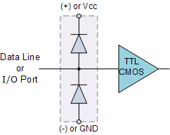
Signal diode arrays can also be used in digital and computer circuits to protect high speed data lines or other input/output parallel ports against electrostatic discharge, (ESD) and voltage transients.
By connecting two diodes in series across the supply rails with the data line connected to their junction as shown, any unwanted transients are quickly dissipated and as the signal diodes are available in 8-fold arrays they can protect eight data lines in a single package.
Signal diode arrays can also be used to connect together diodes in either series or parallel combinations to form voltage regulator or voltage reducing type circuits or even to produce a known fixed reference voltage.
We know that the forward volt drop across a silicon diode is about 0.7v and by connecting together a number of diodes in series the total voltage drop will be the sum of the individual voltage drops of each diode.
However, when signal diodes are connected together in series, the current will be the same for each diode so the maximum forward current must not be exceeded.
Connecting Signal Diodes in Series
Another application for the small signal diode is to create a regulated voltage supply. Diodes are connected together in series to provide a constant DC voltage across the diode combination. The output voltage across the diodes remains constant in spite of changes in the load current drawn from the series combination or changes in the DC power supply voltage that feeds them. Consider the circuit below.
As the forward voltage drop across a silicon diode is almost constant at about 0.7v, while the current through it varies by relatively large amounts, a forward-biased signal diode can make a simple voltage regulating circuit. The individual voltage drops across each diode are subtracted from the supply voltage to leave a certain voltage potential across the load resistor, and in our simple example above this is given as 10v - ( 3*0.7V ) = 7.9V.
This is because each diode has a junction resistance relating to the small signal current flowing through it and the three signal diodes in series will have three times the value of this resistance, along with the load resistance R, forms a voltage divider across the supply.
By adding more diodes in series a greater voltage reduction will occur. Also series connected diodes can be placed in parallel with the load resistor to act as a voltage regulating circuit. Here the voltage applied to the load resistor will be 3*0.7v = 2.1V. We can of course produce the same constant voltage source using a single Zener Diode. Resistor, RD is used to prevent excessive current flowing through the diodes if the load is removed.
Freewheel Diodes
Signal diodes can also be used in a variety of clamping, protection and wave shaping circuits with the most common form of clamping diode circuit being one which uses a diode connected in parallel with a coil or inductive load to prevent damage to the delicate switching circuit by suppressing the voltage spikes and/or transients that are generated when the load is suddenly turned “OFF”. This type of diode is generally known as a “Free Wheeling Diode”, “Flywheel Diode” or simply Freewheel diode as it is more commonly called.The Freewheel diode is used to protect solid state switches such as power transistors and MOSFET’s from damage by reverse battery protection as well as protection from highly inductive loads such as relay coils or motors, and an example of its connection is shown below.
Use of the Freewheel Diode

Modern fast switching, power semiconductor devices require fast switching diodes such as free wheeling diodes to protect them form inductive loads such as motor coils or relay windings. Every time the switching device above is turned “ON”, the freewheel diode changes from a conducting state to a blocking state as it becomes reversed biased.
However, when the device rapidly turns “OFF”, the diode becomes forward biased and the collapse of the energy stored in the coil causes a current to flow through the freewheel diode. Without the protection of the freewheel diode high di/dt currents would occur causing a high voltage spike or transient to flow around the circuit possibly damaging the switching device.
Previously, the operating speed of the semiconductor switching device, either transistor, MOSFET, IGBT or digital has been impaired by the addition of a freewheel diode across the inductive load with Schottky and Zener diodes being used instead in some applications. But during the past few years however, freewheel diodes had regained importance due mainly to their improved reverse-recovery characteristics and the use of super fast semiconductor materials capable at operating at high switching frequencies.
Other types of specialized diodes not included here are Photo-Diodes, PIN Diodes, Tunnel Diodes and Schottky Barrier Diodes. By adding more PN junctions to the basic two layer diode structure, other types of semiconductor devices can be made.
For example a three layer semiconductor device becomes a Transistor, a four layer semiconductor device becomes a Thyristor or Silicon Controlled Rectifier and five layer devices known as Triac’s are also available.
In the next tutorial about diodes, we will look at the large signal diode sometimes called the Power Diode. Power diodes are silicon diodes designed for use in high-voltage, high-current mains rectification circuits.


